Phone: +1 (281) 968-0718
Email: sales@USComponent.com


26
Feb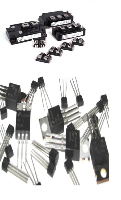
Comparison between IGBT and MOSFET

Metal-Oxide Semiconductor Field Effect Transistor (MOSFET) and Insulated Gate Bipolar Transistor (IGBT) are the two most popular versions among various types of switch-mode power supply (SMPS) transistors are available today. It has been observed that MOSFETs are suitable for low-voltage, low-current and high switching frequencies. On the other hand, IGBTs are favorable for high-voltage, high-current and low switching frequencies.
There may be an argument that on which device works better in SMPS applications, the fact is this: there’s no common norm to specify which device performs better in a particular category of circuit. It differs from application to application, and a wide range of factors, such as speed, size, and cost, all play a role to ordain the exact choice.
Now we are going to enlighten on the differences between these two transistors rather than say that one is better than the other straight away.
The MOSFET is a three-terminal fully-controlled switch. Gate, drain and source are its three terminals. The gate/control signal occurs between the gate and source, and its switch terminals are the drain and source. The gate itself is made of metal. A metal oxide separates it from the source and drain. This grants for reduced power draining and makes MOSFET an excellent option to use as an electronic switch or common-source amplifier.
To operate satisfactorily, a positive temperature coefficient has to be sustained by MOSFETs. As a result of this, there’s little-to-no chance of thermal runaway. On-state losses are lower because the transistor’s on-state-resistance, theoretically speaking, has no limit. Also, MOSFETs can carry through fast switching applications with little turn-off losses because they can function at high frequencies.
The IGBT is also a three terminal (gate, collector, and emitter) full-controlled switch. Its gate/control signal takes place between the gate and emitter, and its switch terminals are the drain and emitter.
The IGBT puts the common gate-drive feature found in the MOSFET with the high-current and low-saturation-voltage capability of a bipolar transistor at the same time. It does this by utilizing an isolated gate field effect transistor for the control input, and a bipolar power transistor as a switch.
Turning on and off rapidly are the specific characteristics of IGBT. Actually its pulse repetition frequency really gets into the ultrasonic extent. This identical ability is why IGBTs are frequently implemented in amplifiers to synthesize complex waveforms with pulse width modulation and low-pass filters. IGBTs are also used to yield big power pulses in fields like particle and plasma physics, and have set up a role in modern appliances like electric cars, trains, elevators, refrigerators, vacuum cleaner etc.
These transistors are very similar in terms of structures. When it comes to electron current flow, a significant difference is the addition of a p-substrate layer beneath the n-substrate layer in the IGBT. In this extra layer, holes are injected into the highly-resistive n-layer, generating a carrier overflow. This increment in conductivity within the n-layer assists to lessen the total on-state voltage of the IGBT. Unfortunately, it also obstructs reverse current flow. As a result, an extra diode (often referred to as a “freewheeling” diode) gets placed parallel with the IGBT to conduct the current in an inverse direction.

USComponent is glad to offer:
- HIGH QUALITY
- FAST DELIVERY
- REASONABLE PRICE
side links
USComponent Inc.
Call us: +1 (281) 968-0718
Email: sales (at) uscomponent.com
Address: 3521 Glisten Street, Norman, OK 73072 USA

this site is ©copyright USComponent 2001-2024, all rights Reserved